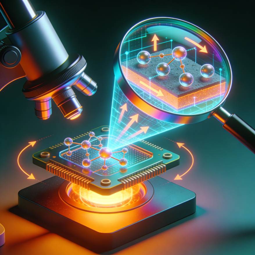
In this study, researchers directly observed moiré transformations in 2D materials by heating twisted bilayer systems. As a result, they captured how atoms rearrange to form stable stacking configurations. Importantly, this work provides a rare atom-level view of moiré pattern evolution. It shows how heat drives structural changes that strongly affect electronic and quantum properties.
Zhang, Y., Baek, J., Lee, C., Jung, Y., Hong, S. C., Nolan, G., Watanabe, K., Taniguchi, T., Lee, G., & Huang, P. Y. conducted this research and published it under the title “Atom-by-atom imaging of moiré transformations in 2D transition metal dichalcogenides. Science Advances” in March 2025.
What the Researchers Achieved in Transformations in 2D Materials
The research team imaged twisted bilayer transition metal dichalcogenides (TMDs), such as MoSe₂/WSe₂, while applying controlled heating. This work directly advances the understanding of transformations in 2D materials at the atomic scale. They used graphene-encapsulated samples placed on specialized heating chips. Short thermal pulses ranging from 100°C to 1000°C triggered structural changes.
During heating, moiré domains nucleated and expanded into aligned regions, highlighting real-time transformations in 2D materials. For example, bilayers twisted at 7.6 degrees transformed into perfectly aligned 0-degree stacks. At the atomic level, the researchers tracked how atoms moved through grain boundaries containing 5|7 topological defects. Therefore, every atomic shift during these transformations in 2D materials was directly observed.

Practical Uses of Transformations in 2D Material
Electronics and Quantum Devices
First, aligned bilayer stacks formed through transformations in 2D materials improve long-term device stability. Next, precise control over moiré patterns ensures consistent electronic behavior.
For instance, applying annealing steps during fabrication can produce uniform moiré structures across large areas. Consequently, technologies such as valleytronics and spintronics benefit from predictable transformations in 2D material. This progress supports the development of faster and more efficient electronic chips.
Sensors and Optoelectronics
Low-energy heat pulses are driving. Transformations in 2D materials can also create localized exciton traps. These structures are valuable for light-emitting diodes, photodetectors, and optical sensors. In addition, certain moiré interfaces exhibit ferroelectric behavior, allowing them to store information.
As a result, flexible electronics and advanced optoelectronic devices gain new design pathways through controlled transformations in 2D material.
Commercial Timeline for Transformations in 2D Materials
From Laboratory to Prototypes
Currently, suitable samples for studying transformations in 2D materials can already be produced using chemical vapor deposition (CVD) methods. In addition, annealing protocols are expected to mature within two to three years.
By 2028, prototype devices using controlled transformations in 2D material may appear. Soon after, quantum sensors based on these materials could follow around 2030. Although large-scale production still requires defect management, progress continues steadily.
Market Deployment
Looking further ahead, fully integrated chips based on engineered transformations in 2D materials may reach the market by 2035. Flexible displays and neuromorphic computing systems are also likely to benefit.
As mass CVD techniques improve, production costs should decline. In the long term, transformations in 2D materials may play a key role in AI hardware and advanced computing platforms.
Research Areas and Career Paths Focused on Transformations in 2D Materials
2D Materials Synthesis
Students can specialize in growing TMD monolayers using CVD techniques. By stacking twisted bilayers, they gain hands-on experience with transformations in 2D materials. Career opportunities exist at major research initiatives such as Graphene Flagship laboratories, startups, and electronics companies like Samsung.
In-situ electron microscopy
Another path involves using in situ STEM imaging during heating experiments. Researchers track grain boundaries and atomic motion frame by frame to study transformations in 2D materials. National laboratories and research institutes actively seek experts with these skills.
Moiré Theory and Simulation
Students interested in theory can model reconstruction energies and domain growth linked to transformations in 2D material. Using density functional theory (DFT), they study stacking faults and predict material behavior. These skills support careers in computational physics and materials modeling.
Device Engineering
Finally, device-focused students can build moiré transistors and evaluate annealing effects driven by transformations in 2D material. Large semiconductor companies seek engineers who can tune twist angles for optoelectronic performance. Often, this work leads to patents and long-term career growth.
Why Transformations in 2D Materials Matter Now
This study captures transformations in 2D materials at the atomic scale as they happen. By revealing how heat reshapes twisted bilayers, it provides a powerful design tool for next-generation electronics and quantum devices.
For students and researchers, Transformations in 2D Material offers rapid innovation at the intersection of physics, materials science, and engineering. Entering this field now means joining one of the most active areas in modern nanotechnology.
Additionally, to present your innovative research and participate in a collaborative learning environment, visit the National Youth Conference on STEM at nycstem.in. Basically, this is our premier platform where we host conferences dedicated to science, technology, engineering, and mathematics. Further, at nycstem.in, you will find a wealth of information regarding our simple four-step process to register, submit your presentation, and receive your official certificate.
Conclusion:Moiré Transformations in 2D Materials
In summary, this research reveals how heat drives atomic-level transformations in 2D materials, allowing twisted bilayers to reorganize into stable structures. These discoveries improve our understanding of moiré patterns and their influence on electronic and quantum properties. As fabrication techniques advance, controlled transformations in 2D materials could enable future quantum devices, advanced electronics, and next-generation computing technologies.
Reference
- Zhang, Y., Baek, J., Lee, C., Jung, Y., Hong, S. C., Nolan, G., Watanabe, K., Taniguchi, T., Lee, G., & Huang, P. Y. (2024). Atom-by-atom imaging of moiré transformations in 2D transition metal dichalcogenides. Science Advances, 10(13), eadk1874.https://doi.org/10.1126/sciadv.adk1874